Customer-Specific Imaging Modules in High-Resolution Image Quality
Jenoptik is a full-service provider that will develop your specific imaging concept for you — from the initial idea to the finished system.

Our high-performance cameras, image processing products and complete OEM systems are ideal for use in the scientific and industrial imaging market: We supply imaging modules both for high-volume projects and for individual projects.
We tailor all of our products to your precise requirements— with a complete value chain: from sensors and sensor boards through to camera system solutions with our own firmware for your specific application.
We optimize the basic version of our compact CMOS USB camera module for your needs. With a 5-megapixel resolution and a USB 2.0 interface, this module provides the ideal platform. We can deliver customer-specific modifications within a very short turnaround time. We can also make minor changes to the hardware and software or build complete systems from different modules for your image processing applications.
For more complex projects, we can combine the properties and features of our camera module according to your requirements.
They include:
We also support you by offering professional supply chain management, and take care of the entire value chain for you. We maintain a clear overview of the whole process, and ensure that you are able to bring your product to market quickly, helping you to secure sustainable success.
We tailor all of our products to your precise requirements— with a complete value chain: from sensors and sensor boards through to camera system solutions with our own firmware for your specific application.
We optimize the basic version of our compact CMOS USB camera module for your needs. With a 5-megapixel resolution and a USB 2.0 interface, this module provides the ideal platform. We can deliver customer-specific modifications within a very short turnaround time. We can also make minor changes to the hardware and software or build complete systems from different modules for your image processing applications.
For more complex projects, we can combine the properties and features of our camera module according to your requirements.
They include:
- Form factor.
- Resolution (1 MP, 3 MP, 5 MP, 10 MP, 14 MP, ...).
- Sensor type (CCD / CMOS).
- Digital interface (USB 2.0, USB 3.0).
- Optical interface (C-mount, S-mount, CS-mount).
- Optics, filters and more.
Expertise for Successful Imaging Modules
We deliver imaging modules that help you achieve success. Jenoptik experts are on hand to support you throughout your project, and work together with you as system partner: We take care of the design process, andperform feasibility studies, as well as devising the OEM camera design. This allows us to produce prototypes and deliver your imaging solutions in the shortest possible time.We also support you by offering professional supply chain management, and take care of the entire value chain for you. We maintain a clear overview of the whole process, and ensure that you are able to bring your product to market quickly, helping you to secure sustainable success.
Our Expertise
- 17 years of know-how in the production of opto-electronic systems
- Unique selling point: Inline LED module measurement technology
- Rapid Protoyping
- Design for Manufacturing
- Well-founded advice on product development, qualification and series transition
ISO Certificates
- DIN EN ISO 9001 (QM-System)
- DIN EN ISO 13485 (Medical Application)
- ISO 14001 (Environment Management System)
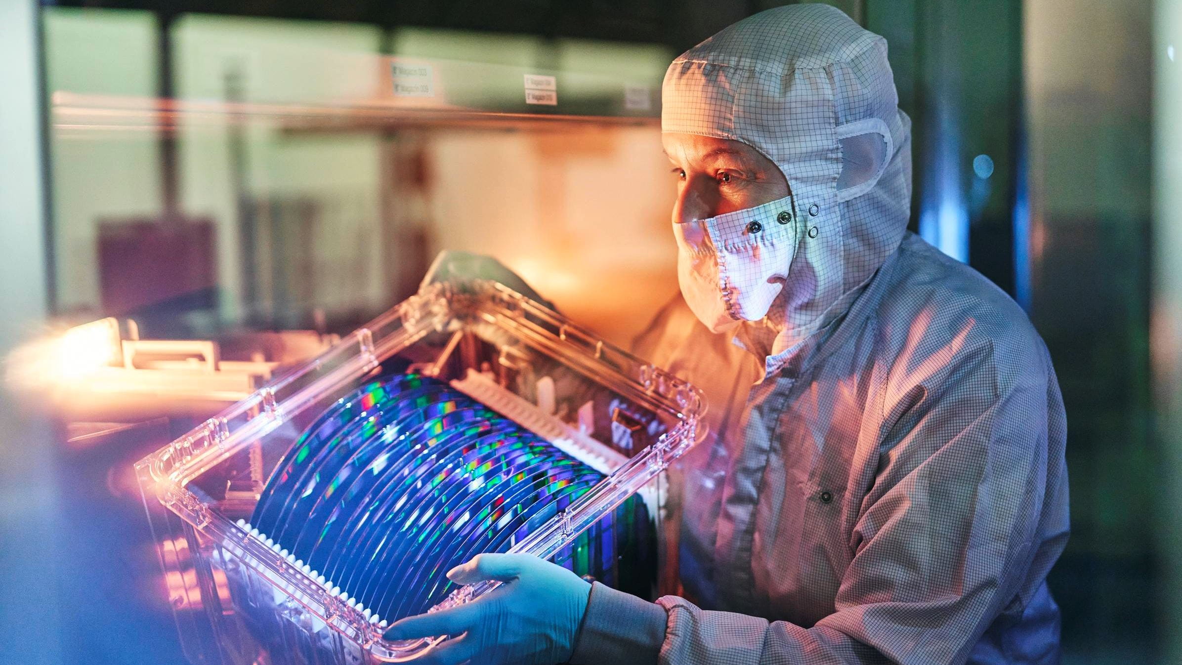
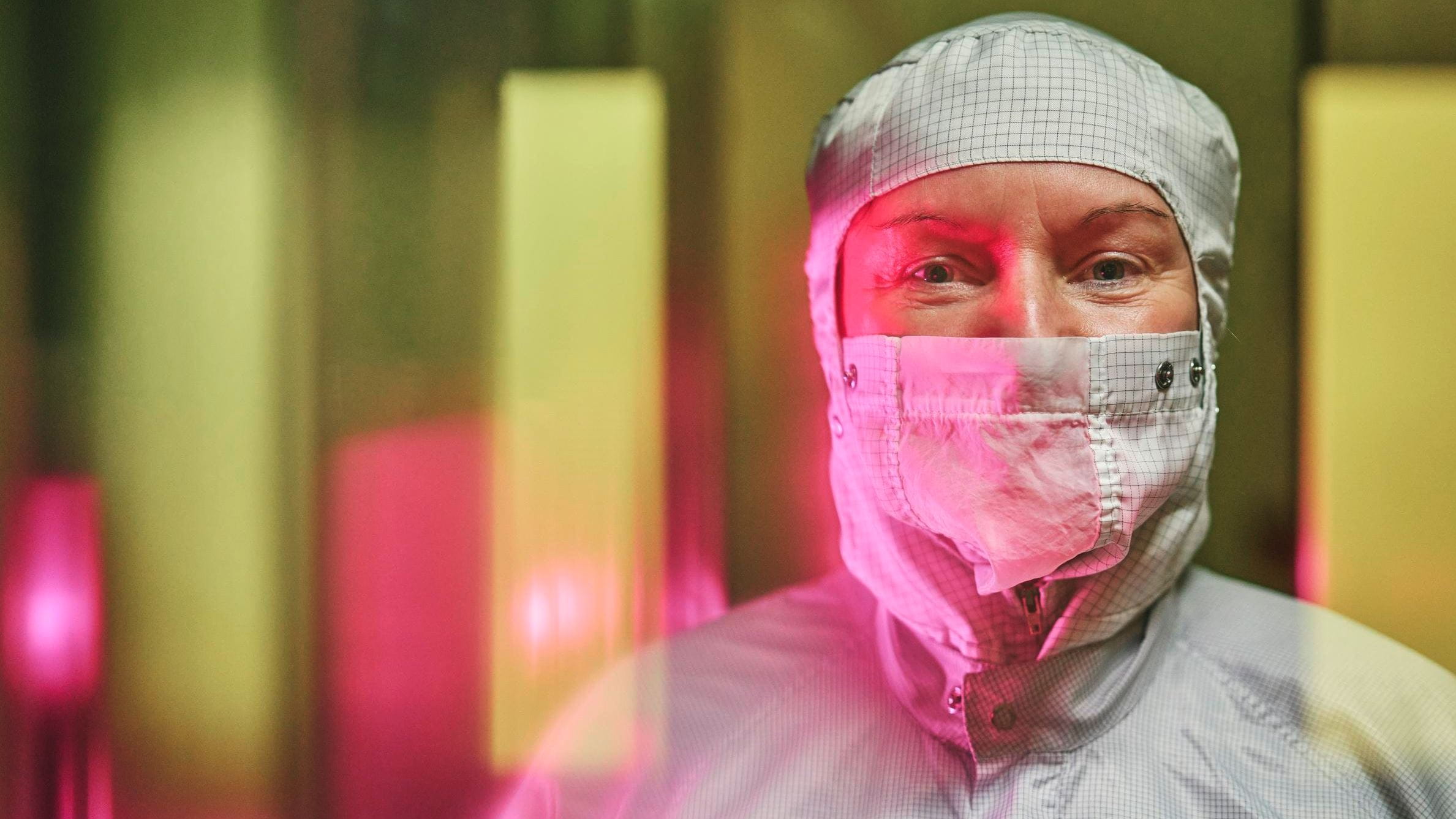
Department Production Information
- Department exists since 2006 at Jenoptik
- Area: approx. 400m²
Area consists of two clean room classes:
- 2/3 of the area ISO class 5 (max. 832 particles with 1 µm/m³)
- 1/3 of the surface ISO class 7 (max. 83,200 particles with 1 µm/m³)
Process steps in detail

Learn more about our core competencies for customer imaging modules
Dicing
Die-Bonding
Wire-Bonding
Housing
Testing
Separation
Core competence Dicing

Semiconductor Wafer
Substrate sizes
- Diameter up to 12 inches
- Thickness 0.1mm to 5mm
- Accuracy: up to 2 µm
Creation of negative 3D structures
- Increase adhesive surface for later bonding
- Change reflection characteristics
Full underwater separation option with following benefits
- Increase purity
- ESD safety through conductance controlled ultrapure water
Separable Materials
- Ceramics and sintered ceramics
- PCB materials / metals
- Composite materials and plastics
- Silicon / glass
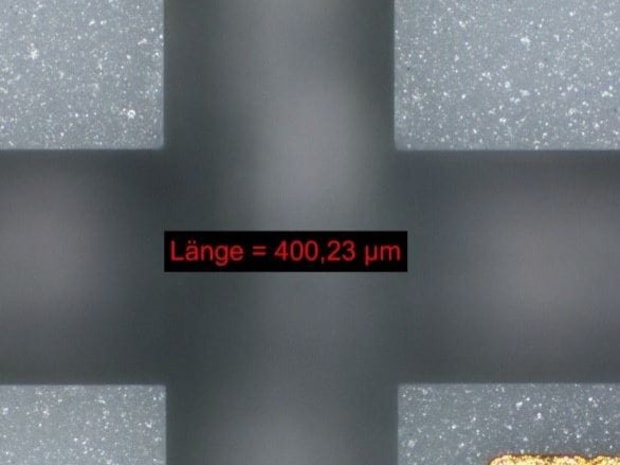
Application Examples for Dicing
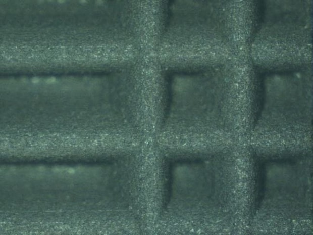
3D structure to increase adhesive surface (180µm)
Cut in sintered ceramics
Core competencies Die-Bonding
Full Format Image Sensor (Au, Ball-Wedge, 25µm)
Technology
- Adhesive die bonding (inline dispensing & stamping)
- Sintering
- Stacked die bonding
- Flip chip technology
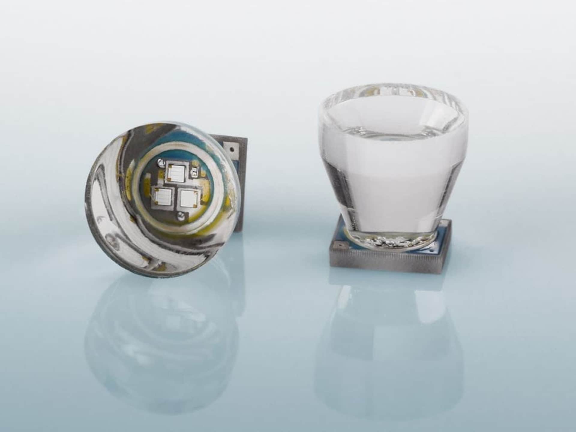
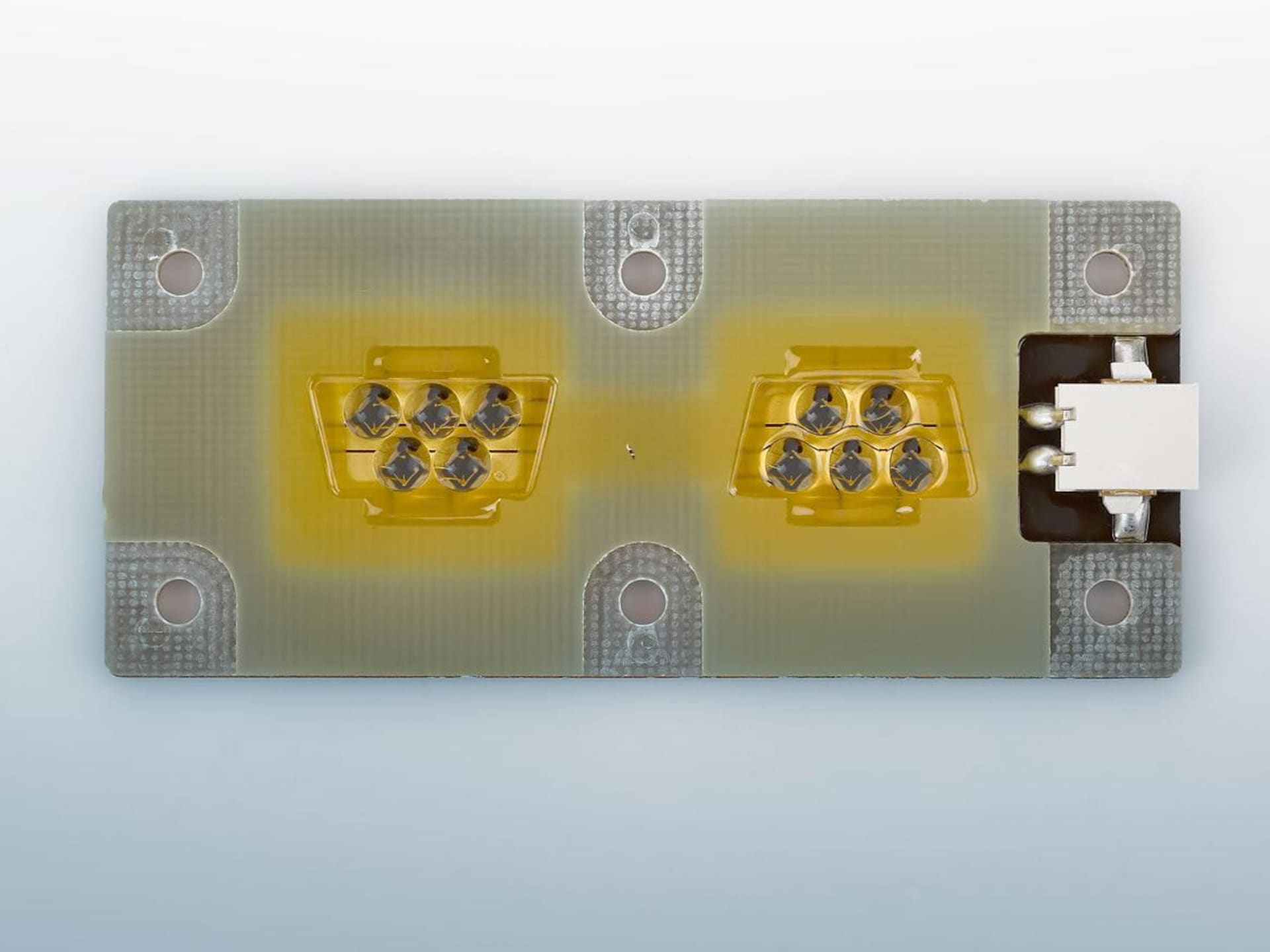
Applications
- Wafer-level packaging (WLP) of MEMS and sensors
- Flip chip
- LED modules
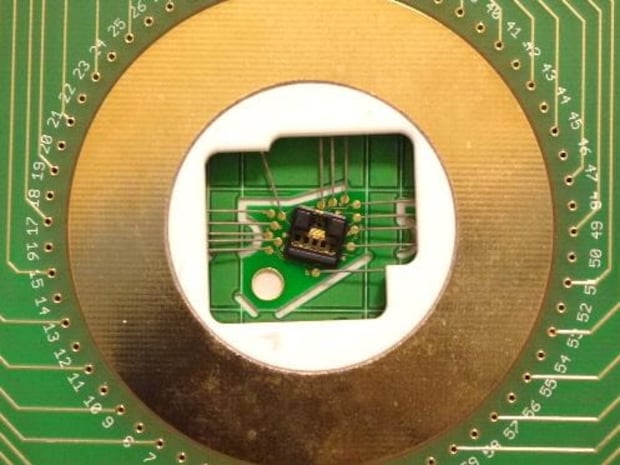
- Image sensors
- Handling of image sensor with micro lens arrys
Substrates
- Circuit boards, wafers, component carriers, lead frames
Component dimensions
- 0.17mm up to 50mm
- > 25µm thickness
- Accuracy up to < 5µm
Component feed options:
- Wafer, waffle / Gel-Pak, reel
Marking
Technology
- Laser marking
- Printing system (Ink Jet)
Applications
- Traceability
Cleaning
Technology
- barrel reactor
Applications
- Clean organic residues from surface
- Activate surface (increase adhesion forces during joining processes)
Core Competence Wire-bonding
Technology
- Wedge-Wedge and Ball-Wedge
- Accuracy bond tool: 2.5 µm
- Wire diameter: 12.5 µm up to 75 µm
- Material: gold, aluminum, silver, copper, and platinum
Core competence
- Adjust loop profile for ultra flat bonds
- Reflection-poor ball-wedge technology
Core competence Housing: Dispensing
Technology
- Accuracy 14µm
- Volume- or mass-controlled dispensing
- Volume accuracy: 0.1µl
Materials
- Silicone (in different cleanroom)
- 2/3K epoxy, polyurethane
Special competences
- Dam fill / underfill
- Black encapsulation to reduce reflections
- Mechanical protection
- Optical encapsulation to change light parameter
Core competence Housing: Set and seal optics
- Accuracy (regarding die-bonding) < 5µm
- Processing of special epoxy resins
- Minimization of trapped air (special evacuation procedure)
- Cavity flushing with N2 during the setting process
- Curing of potting with temperature or UV light
Core competence: EOL-Test
Opto-electrical measurement and AOI, contacting with card according to customer design
Probing-Station
- Accuracy up to 3µm
- Current-voltage characteristics
- 40W Current/voltage source with 4-point measurement
- Radiant intensity and wavelength measurement
- Automatic optical inspection (AOI)
- Applicatio12 MP Camera
- Switching/multiplexing with up to 32 contacts
- Logic measurements, multi-segment displays, etc.
- Flying probe
Further Product Recommendations

Do you have any questions? Our experts are happy to help.


Digital Imaging & Optoelectronic Systems
HCI-CN-Carl-Wang
EditContact
Sales North America